Wamkelekile, Welkom
Award for UCT nanovators at Silicon Valley
09 January 2012 | Story by Newsroom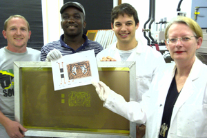 Burning bright: (From left) UCT NanoSciences Innovation Centre's Prof Margit Harting (right) and students Ulrich Mannl, Batsirai Magunje and Stanley Walton show off a newly printed tiger design large area temperature sensor, produced in collaboration with Austin-based company Novacentrix, using their unique copper ink and processing methods. The design is the first step towards replacing expensive - and ecologically questionable - silver inks. For this and other innovations, UCT's nanovators won the recent 2011 Printed Electronics USA Best in Show Award.
The Department of Physics' NanoSciences Innovation Centre and their spin-out nanotechnology company, PST Sensors, scooped the Printed Electronics USA Best in Show Award at the recent 2011 Printed Electronics USA Conference in Silicon Valley.
This is their second major award, following on the heels of their 2010 Printed Electronics Europe Academic R&D Award.
The Silicon Valley event is reported to have been the largest-ever global printed electronics conference. But it was UCT and PST Sensors' joint innovative developments in thermal imaging and sensor imaging technology that stole the show.
The show-stopper was a large-area temperature sensor in the guise of a decorative graphic.
Professor David Britton, co-director of the NanoSciences Innovation Centre, explained: "The large-area sensor looks like a novelty gimmick, with the active sensor printed in the form of a graphic design, a zebra for example, using silver ink for the contacts with the black silicon nanoparticle ink for the active semiconductor, or even a tiger, using a copper ink."
Their decorative appeal camouflages their usefulness. Conventional electronic temperature sensors are small, bead-like devices that can measure temperature at a specific point only. These large-area sensors can be printed onto a container (or even wrapped around a container) to measure the average temperature over a large volume.
"The averaging over a large area makes the temperature reading more stable, avoiding the influence of hot or cold spots and poor thermal contact with the object whose temperature is being measured," said Britton. "Imagine the temperature of a fridge or incubator, or even a room, being measured on all the walls at the same time instead of at one position near the door."
The potential is huge for the packaging and retail sectors, transport and logistics, aerospace and automotive engineering, healthcare, and marketing and advertising.
The UCT group is working with a major international company on applications in food and pharmaceutical packaging, where safety is an important concern.
Also on display at the Silicon Valley conference was the team's thermal-imaging mat.
Like infra-red cameras, this device produces a picture of an object's temperature profile, but unlike a camera, it doesn't need a clear line of sight.
"For many applications we need to know not only the average temperature, but its distribution," said Britton. "This isn't possible using conventional sensors, especially over a large area or an oddly shaped surface."
Its applications in advanced engineering are legion, particularly in the aerospace sector where engineers need to pinpoint temperature distribution in airframes or engine housing. There is also great potential in chemical processing and in nuclear engineering where these devices monitor the process in a reactor vessel.
"We're investigating uses in health care and the NanoSciences Innovation Centre is working with a broader consortium that includes members of the Faculty of Health Sciences," added Britton.
All 1 500 registered delegates received their own printed temperature sensor, (designed as electronic components to be put into temperature sensing/monitoring circuits), courtesy of IDTEchEx, PST Sensors and the UCT NanoSciences Innovation Centre.
"For the nanovators, exhibiting at conferences like Printed Electronics USA is a fun reward for their research efforts, and allows them to meet scientists, engineers and business people at all levels and from all disciplines," said Britton.
"We can show the rest of the world that UCT is not only a globally competitive research institution and that Cape Town is a centre of innovation that is leading the world in silicon nanotechnology, but that they are an important part of it."
The centre's research work covers all aspects of nanotechnology, from the basic science of nanoparticle surface, through studies of electronic properties, to the development of prototypes for applications in sensors, electronics and, increasingly importantly, solar power where the NanoSciences Innovation Centre is leading a USAID funded research network, Nano Power Africa.
 This work is licensed under a Creative Commons Attribution-NoDerivatives 4.0 International License.
Please view the republishing articles page for more information.